2�
� RF Device Data�
� Freescale Semiconductor�
� MRF6S19140HR3 MRF6S19140HSR3�
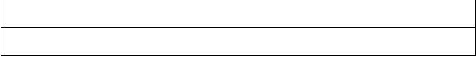
� Table 3. ESD Protection Characteristics�
� Test Methodology�
� Class�
� Human Body Model (per JESD22-A114)�
� 2 (Minimum)�
� Machine Model (per EIA/JESD22-A115)�
� A (Minimum)�
� Charge Device Model (per JESD22-C101)�
� IV (Minimum)�
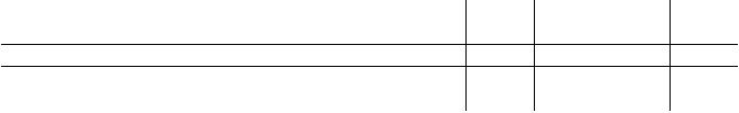
� Table 4. Electrical Characteristics (TC�
� = 25�
� °C unless otherwise noted)�
� Characteristic�
� Symbol�
� Min�
� Typ�
� Max�
� Unit�
� Off Characteristics�
� Zero Gate Voltage Drain Leakage Current�
� (VDS�
� = 68 Vdc, V�
� GS�
� = 0 Vdc)�
� IDSS�
� ?�
� ?�
� 10�
� μAdc�
� Zero Gate Voltage Drain Leakage Current�
� (VDS�
� = 28 Vdc, V�
� GS�
� = 0 Vdc)�
� IDSS�
� ?�
� ?�
� 1�
� μAdc�
� Gate-Source Leakage Current�
� (VGS�
� = 5 Vdc, V�
� DS�
� = 0 Vdc)�
� IGSS�
� ?�
� ?�
� 1�
� μAdc�
� On Characteristics�
� Gate Threshold Voltage�
� (VDS�
� = 10 Vdc, I�
� D�
� = 300 �
� μAdc)�
� VGS(th)�
� 1�
� 2�
� 3�
� Vdc�
� Gate Quiescent Voltage�
� (VDD�
� = 28 Vdc, I�
� D�
� = 1150 mAdc, Measured in Functional Test)�
� VGS(Q)�
� 2�
� 2.8�
� 4�
� Vdc�
� Drain-Source On-Voltage�
� (VGS�
� = 10 Vdc, I�
� D�
� = 3 Adc)�
� VDS(on)�
� 0.1�
� 0.21�
� 0.3�
� Vdc�
� Dynamic Characteristics�
� (1)�
� Reverse Transfer Capacitance�
� (VDS�
� = 28 Vdc �
� ±�
� 30 mV(rms)ac @ 1 MHz, V�
� GS�
� = 0 Vdc)�
� Crss�
� ?�
� 2�
� ?�
� pF�
� Functional Tests�
� (In Freescale Test Fixture, 50 ohm system) V�
� DD�
� = 28 Vdc, I�
� DQ�
� = 1150 mA, P�
� out�
� = 29 W Avg., f1 = 1930 MHz, �
� f2 = 1932.5 MHz and f1 = 1987.5 MHz, f2 = 1990 MHz, 2-carrier N-CDMA, 1.2288 MHz Channel Bandwidth Carriers. ACPR measured in �
� 30 kHz Channel Bandwidth @ ±885 kHz Offset. IM3 measured in 1.2288 MHz Channel Bandwidth @ ±2.5 MHz Offset. PAR = 9.8 dB @�
� 0.01% Probability on CCDF.�
� Power Gain�
� Gps�
� 15�
� 16�
� 18�
� dB�
� Drain Efficiency�
� ηD�
� 26�
� 27.5�
� ?�
� %�
� Intermodulation Distortion�
� IM3�
� ?�
� -37�
� -35�
� dBc�
� Adjacent Channel Power Ratio�
� ACPR�
� ?�
� -51�
� -48�
� dBc�
� Input Return Loss�
� IRL�
� ?�
� -15�
� -9�
� dB�
� 1. Part is internally matched both on input and output.�
�  �
�
� � �  �
�
� � �  �
�
� � �  �
�
� � �  �
�
� � �  �
�
� � �  �
�
� � �  �
�
� � 发布紧急采购,3分钟左右您将得到回复。
相关PDF资料
MRF6S19200HSR5
MOSFET RF N-CH 56W 28V NI780S
MRF6S20010GNR1
MOSFT RF N-CH 28V 10W TO270-2 GW
MRF6S21050LSR5
MOSFET RF N-CH 28V 11.5W NI-400S
MRF6S21060NR1
MOSFET RF N-CH 28V 14W TO270-4
MRF6S21100HSR5
MOSFET RF N-CHAN 28V 23W NI-780S
MRF6S21100NR1
MOSFET RF N-CH 28V 23W TO270-4
MRF6S21140HSR5
MOSFET RF N-CHAN 28V 30W NI-880S
MRF6S21190HSR5
MOSFET RF N-CH 54W NI880S
相关代理商/技术参数
MRF6S19200H
制造商:FREESCALE 制造商全称:Freescale Semiconductor, Inc 功能描述:RF Power Field Effect Transistors
MRF6S19200HR3
功能描述:射频MOSFET电源晶体管 HV6 1.9GHZ 56W 28V NI780 RoHS:否 制造商:Freescale Semiconductor 配置:Single 晶体管极性: 频率:1800 MHz to 2000 MHz 增益:27 dB 输出功率:100 W 汲极/源极击穿电压: 漏极连续电流: 闸/源击穿电压: 最大工作温度: 封装 / 箱体:NI-780-4 封装:Tray
MRF6S19200HR5
功能描述:射频MOSFET电源晶体管 HV6 1.9GHZ 56W 28V NI780 RoHS:否 制造商:Freescale Semiconductor 配置:Single 晶体管极性: 频率:1800 MHz to 2000 MHz 增益:27 dB 输出功率:100 W 汲极/源极击穿电压: 漏极连续电流: 闸/源击穿电压: 最大工作温度: 封装 / 箱体:NI-780-4 封装:Tray
MRF6S19200HSR3
功能描述:射频MOSFET电源晶体管 HV6 1.9GHZ 56W 28V NI780S RoHS:否 制造商:Freescale Semiconductor 配置:Single 晶体管极性: 频率:1800 MHz to 2000 MHz 增益:27 dB 输出功率:100 W 汲极/源极击穿电压: 漏极连续电流: 闸/源击穿电压: 最大工作温度: 封装 / 箱体:NI-780-4 封装:Tray
MRF6S19200HSR5
功能描述:射频MOSFET电源晶体管 HV6 1.9GHZ 56W 28V RoHS:否 制造商:Freescale Semiconductor 配置:Single 晶体管极性: 频率:1800 MHz to 2000 MHz 增益:27 dB 输出功率:100 W 汲极/源极击穿电压: 漏极连续电流: 闸/源击穿电压: 最大工作温度: 封装 / 箱体:NI-780-4 封装:Tray
MRF6S20010GNR1
功能描述:射频MOSFET电源晶体管 HV6 2GHZ 10W RoHS:否 制造商:Freescale Semiconductor 配置:Single 晶体管极性: 频率:1800 MHz to 2000 MHz 增益:27 dB 输出功率:100 W 汲极/源极击穿电压: 漏极连续电流: 闸/源击穿电压: 最大工作温度: 封装 / 箱体:NI-780-4 封装:Tray
MRF6S20010GNR1-CUT TAPE
制造商:Freescale 功能描述:MRF6S20010 Series 1.6 to 2.2 GHz 28 V 10 W RF Power N-Ch Mosfet - TO-270
MRF6S20010NR1
功能描述:射频MOSFET电源晶体管 HV6 2GHZ 10W TO270-2 RoHS:否 制造商:Freescale Semiconductor 配置:Single 晶体管极性: 频率:1800 MHz to 2000 MHz 增益:27 dB 输出功率:100 W 汲极/源极击穿电压: 漏极连续电流: 闸/源击穿电压: 最大工作温度: 封装 / 箱体:NI-780-4 封装:Tray